Researchers at the National Institute of Standards and Technology (NIST) have revived and improved a once-reliable technique to identify and count defects in transistors, the building blocks of modern electronic devices such as smartphones and computers. Over the past decade, transistor components have become so small in high-performance computer chips that the popular method, known as charge pumping, could no longer count defects accurately. NIST’s new and improved method is sensitive enough for the most modern, minuscule technology, and can provide an accurate assessment of defects that could otherwise impair the performance of transistors and limit the reliability of the chips in which they reside.
The new, modified charge pumping technique can detect single defects as small as the diameter of a hydrogen atom (one-tenth of a billionth of a meter) and can indicate where they’re located in the transistor. Researchers could also use the new capability to detect and manipulate a property in each electron known as quantum spin. The ability to manipulate individual spins has applications in both basic research and quantum engineering and computing.
Transistors act as electrical switches. In the on position, which represents the “1” of binary digital information, a designated amount of current flows from one side of a semiconductor to the other. In the off position, representing the “0” of binary logic, current ceases to flow.
Defects in a transistor can interfere with the reliable flow of current and significantly degrade the performance of transistors. These defects could be broken chemical bonds in the transistor material. Or they could be atomic impurities that trap electrons in the material. Scientists have devised several ways to categorize defects and minimize their impact, tailored to the structure of the transistor under study.
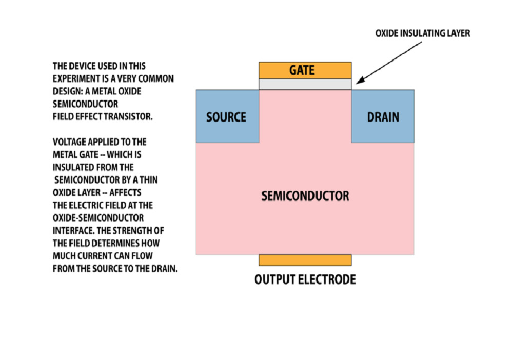
In the traditional design known as the metal oxide semiconductor field effect transistor (MOSFET), a metal electrode called the gate sits atop a thin insulating layer of silicon dioxide. Below the insulating layer lies the interface region that separates the insulating layer and the main body of the semiconductor. In a typical transistor, current travels through a narrow channel, only one billionth of a meter thick, that extends from the source, which lies on one side of the gate, to a “drain” on the other side. The gate controls the amount of current in the channel.


